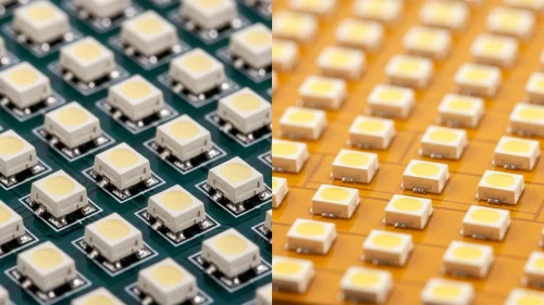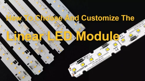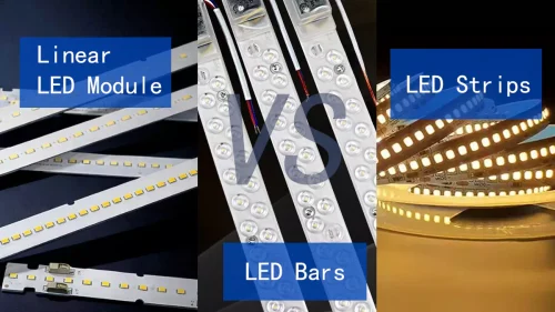
An SMD LED is a compact surface-mount light-emitting diode designed to sit flat on a printed circuit board and be soldered directly to its pads, without the long metal leads used by through-hole packages. The package normally combines an LED die, electrical connections, a reflective or molded housing, phosphor and encapsulant, and solder pads. Its small size supports dense or distributed layouts, while brightness and efficacy depend on the exact die, package construction, drive current, and thermal conditions. A pick-and-place machine positions each device, and reflow soldering forms the electrical and thermal connection to the PCB.
This structure gives the module designer control over LED count, spacing, series-parallel circuits, board shape, and color channels. The same assembly method can support a narrow linear board, a large panel, a circular module, or a tunable-white light engine. Individual SMD packages remain separate points of light, so spacing and secondary optics determine whether the finished fixture shows hotspots, multiple shadows, or a smooth luminous surface.
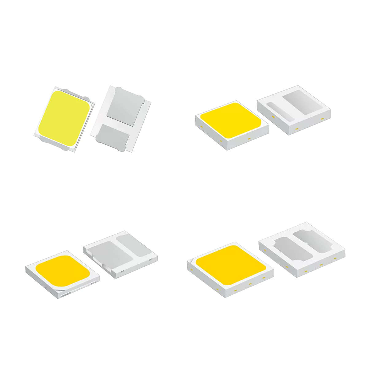
Common four-digit names usually describe the nominal package outline in tenths of a millimeter. A 2835 package is about 2.8 by 3.5 mm, while a 3030 is about 3.0 by 3.0 mm. The code is a footprint clue, not a performance grade. Two LEDs with the same outline can have different die structures, voltages, power ratings, thermal resistance, CRI, sulfur resistance, and LM-80 data. Lumileds, for example, lists multiple 2835 and 3030 families for different commercial, architectural, color, and environmental requirements.
Common SMD family | Nominal outline | Typical lighting role | What the code does not confirm |
|---|---|---|---|
2835 | 2.8 x 3.5 mm | Linear modules, panels, troffers, bulbs, and distributed general lighting | Power, efficacy, CRI, voltage, lifetime, or environmental robustness |
3030 | 3.0 x 3.0 mm | Commercial, outdoor, horticultural, and higher-load module designs | Whether the device is suitable for heat, humidity, sulfur, or a specific drive current |
3535 | 3.5 x 3.5 mm | Higher-power white or color applications and tighter optical control | Beam, die type, thermal path, or color channel configuration |
5050 | 5.0 x 5.0 mm | Higher-flux white packages, RGB/RGBW products, and outdoor modules | Number of dies, circuit arrangement, voltage, or actual lumen output |
Note: The table lists common SMD package families only. Non-standard outlines, electrical configurations, spectral options, and application-specific packages are also available; final selection must use the exact part number and datasheet.
Our self-developed high-efficiency LED chips are also based on several mainstream chip size specifications. Therefore, when developing production solutions for customers, we start with a complete BOM and datasheet, not just “2835 and 3030”. In Higntek’s engineering work, we precisely match LEDs with target efficiency, color temperature, color rendering index, voltage, and current, and then check PCB layout, heat dissipation paths, optics, and manufacturability according to the customer’s luminaire requirements.
COB LED stands for Chip on Board LED. A COB LED mounts multiple bare LED dies directly onto a shared substrate and connects them as one light source. A common silicone-phosphor layer forms one defined light-emitting surface, often called the LES, so the fixture can be designed around a single optical center. The COB is then mounted through a holder or interface to a heat sink and paired with a reflector or lens sized for the actual LES.
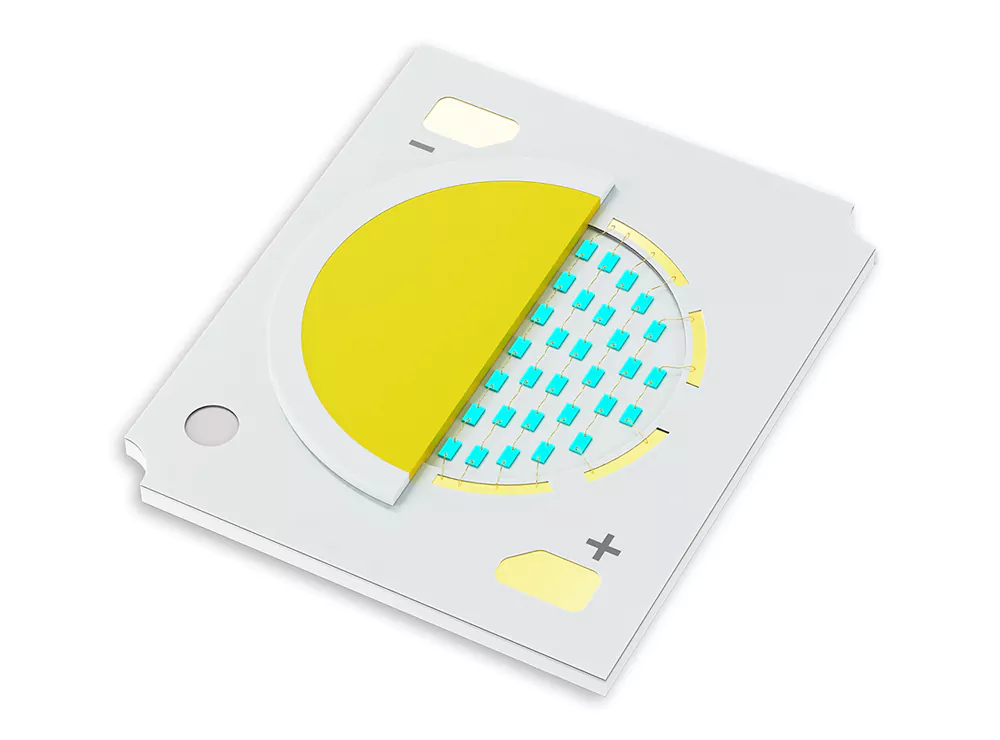
The U.S. Department of Energy’s study of commercial COB products describes the platform as many interconnected mid-power dies arranged into a dense emitting surface. That density produces substantial light and waste heat in a small area, which is why the substrate and the complete path from COB case to ambient air require deliberate thermal design.
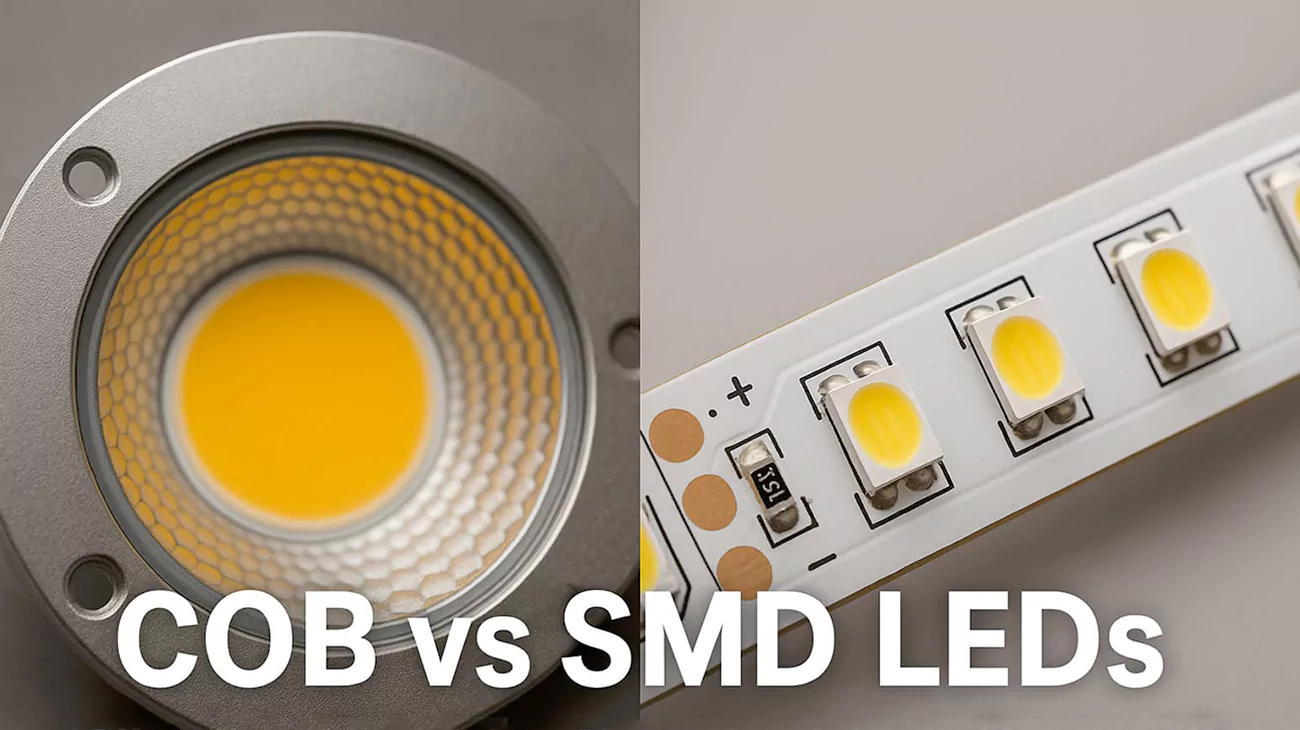
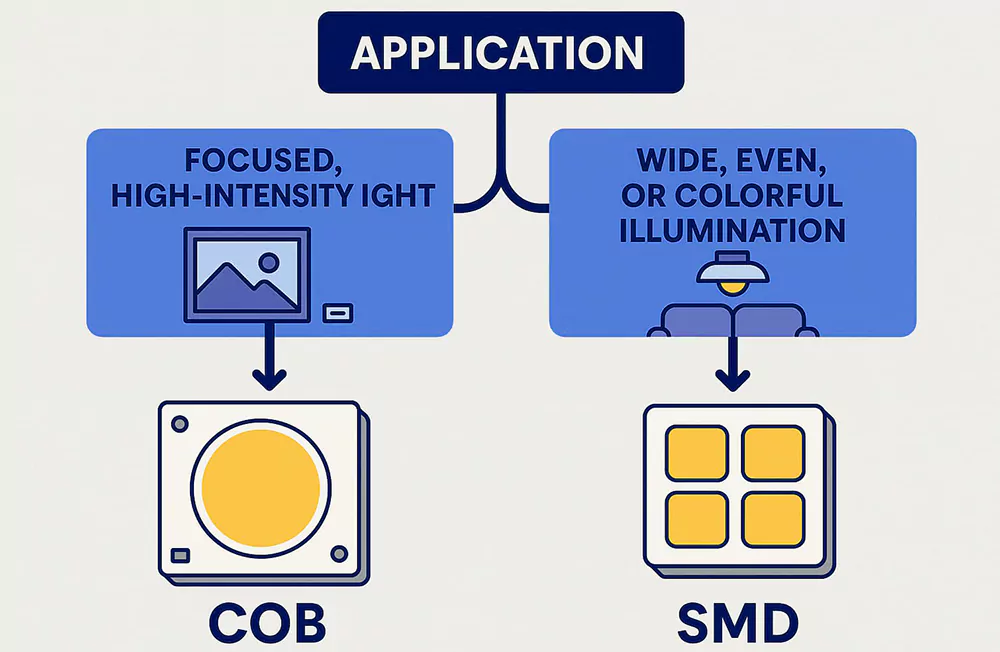
COB and SMD LED packaging technologies differ in their unit of integration. SMD uses individually packaged LEDs assembled onto a PCB, while COB integrates many bare dies on one shared substrate before the light source enters the fixture. That structural choice changes layout freedom, heat concentration, optics, assembly, sourcing, and service strategy.
Source Structure.
Source structure is the first difference, and it decides where the design freedom lives. An SMD light engine is built from individually packaged LEDs soldered to a PCB, so the board defines the source: its outline, its series-parallel circuits, and its spacing. A COB bonds many bare dies to one shared substrate under a common phosphor layer, so the source is defined at the die-array level before it meets a fixture. In practice, SMD puts the layout decisions at board level, while COB commits the design to a fixed emitting area from the start.
Light Emitting Point.
Light-emitting geometry follows directly from that unit of integration. SMD emits from many separate points whose spacing the designer controls, which suits panels, troffers, and linear products where a diffuser or mixing chamber builds a smooth luminous surface. COB emits from one compact, continuous light-emitting surface (LES), which suits a single reflector or lens that must control a concentrated source. The practical question is whether the fixture wants many controllable sources or one optical center.
Optical Design.
Optical design should be chosen with the package, not after it. Because SMD sources are distributed, diffusers, lenses, reflectors, and mixing chambers can work across many points, and spacing can be tuned for a given optical cavity. Because COB concentrates light in one LES, a single reflector or lens can form the beam efficiently, but the LES size and the optic must be matched. A shallow fixture with a wide emitting area tends to favor SMD optics; a fixture built around a narrow beam tends to favor one optic on a COB.
Thermal Path.
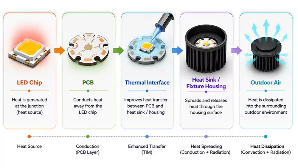
The thermal path starts at the die but ends in the ambient, and the package changes only part of it. SMD adds package and solder-joint interfaces, yet lets the designer spread heat sources across a long or wide PCB and reduce local heat flux. COB removes some internal interfaces because the dies sit directly on a shared substrate, but it concentrates heat in a small footprint, so the holder, thermal interface, heat sink, and airflow must remove more heat per unit area. In both cases the full chain from junction to ambient sets the operating temperature, so the module and fixture need a system-level thermal review rather than a package-level guess.
Design Flexibility.
Layout and channel flexibility is where SMD is hardest to beat. Because the PCB carries the source, the designer can change board shape, series-parallel voltage, CCT, RGB or RGBW channels, and control zones without changing the package. A COB usually arrives with a defined LES, voltage, current, and channel configuration, so reusing it across a product family means revalidating the array. If the roadmap needs several lengths, outputs, or color configurations from one platform, SMD provides that reuse; if every product is a dedicated compact source, the COB’s fixed configuration is less of a constraint.
Production Costs.
Assembly economics differ more in counting than in principle. SMD uses mature SMT placement and reflow, but a large module carries many placements, solder joints, and inspection points. COB reduces source placements at fixture assembly, but it adds a holder and thermal interface step and requires handling the array as one larger component. Which approach wins on cost depends on volume, equipment, board, optics, and heat sink, so the comparison should be made at module and fixture level rather than from package price alone.
Secondary Maintenance.
Repair and redesign behavior also differs. An SMD board can be redesigned around alternate packages, spacing, or layouts, and second sourcing is easier because the package market is broad, although field-level LED repair remains specialized. A COB is normally treated as one replaceable source, so the common service action is whole-array replacement. That is acceptable when the fixture is built around a standard holder, but it leaves fewer options to repair or reconfigure in the field.
Practical Lighting Applications are far more helpful in making effective choices than any generic winning label. SMD fits linear modules, panels, troffers, backlights, strips, tunable systems, and distributed area lighting, and with controlled spacing and matched optics it can also serve downlights, spotlights, track lights, and compact high-bay modules. COB fits the same compact optical architectures when a small LES and one aligned optic are the driving requirement. Match the package to the fixture’s emitting-area and beam needs, then compare specific devices at the same operating point.
Decision factor | SMD LED packaging | COB LED packaging | Practical implication |
|---|---|---|---|
Source structure | Separate packaged LEDs mounted on a PCB | Multiple bare dies on one shared substrate under a common phosphor layer | SMD distributes sources; COB concentrates them |
Light-emitting geometry | Multiple points with designer-controlled spacing | One compact, continuous LES | SMD fits panels and linear layouts; COB fits single-reflector systems |
Optical design | Diffusers, lenses, reflectors, or mixing chambers can work across many sources | One reflector or lens can control the central source efficiently | Optical architecture should be selected with the package, not after it |
Thermal path | Die, package, solder joint, PCB, interface, heat sink, ambient | Die, shared substrate, interface, heat sink, ambient | COB shortens some internal paths but raises local heat flux |
Layout and channels | High freedom for board shape, voltage, CCT, RGB/RGBW, and zoning | Usually a defined LES, voltage, current, and channel configuration | SMD is easier to reuse across a configurable module family |
Assembly | Mature SMT placement and reflow, but more component placements | Fewer source placements at fixture assembly, with holder and TIM requirements | Total cost depends on volume, equipment, board, optics, and heat sink |
Repair and redesign | A board can be redesigned around alternate packages or layouts; field-level LED repair is still specialized | Whole-source replacement is the common service action | SMD generally offers more sourcing and design alternatives |
Typical lighting fit | Linear modules, panels, troffers, backlights, strips, tunable systems, and distributed area lighting | Downlights, spotlights, track lights, compact high-bay sources, and focused beams | Application geometry is a better selector than a generic winner label |
These are architectural tendencies, not guaranteed specifications. Before accepting a comparison, confirm whether each value refers to the bare LED source, the module, or the complete fixture. Then compare the same input power, CCT, CRI, stabilized temperature, driver efficiency, and optical losses. A high-quality SMD package can outperform a COB at one operating point, while another COB can outperform the selected SMD under different conditions.
If your team is comparing SMD and COB for a defined fixture, we can review the target lumens, board envelope, CCT, CRI, drive conditions, thermal path, and optical geometry against the application. Share those constraints with us before locking the package.
Neither SMD nor COB is universally better. SMD is usually the stronger starting point for distributed, configurable lighting modules, while COB is often better for compact fixtures that need high luminous flux from a small light-emitting surface and one focused optical system. The right choice depends on the fixture geometry, target output, thermal path, optical design, electrical configuration, service method, and total cost.
Compare Efficacy at the Real Operating Point.
Package names do not establish luminous efficacy. Compare candidate parts at the required CCT and CRI, then normalize drive current, stabilized junction or case temperature, driver efficiency, and optical losses. Also separate total lumens from beam intensity: a compact COB may produce higher center-beam candela through a matched reflector even when an SMD array delivers similar or greater total lumens. Higher current density can reduce LED efficacy through current and thermal droop, and the finished module or fixture loses additional light in diffusers, lenses, reflectors, and other optical layers.
For an SMD design, distributing the target lumens across more efficiently driven packages may improve efficacy and reduce local thermal stress, but it adds placements and board area. For a COB design, a compact source may simplify optical coupling, but high flux density can demand a larger heat sink. The useful comparison is delivered fixture output per input watt under steady-state conditions, not the maximum package value printed at a favorable test point.
Compare the Complete Thermal Resistance Chain.
COB is not automatically cooler. The package can provide a direct route from die to a thermally conductive substrate, yet many dies release heat through one small area. SMD has additional package and solder interfaces, but the sources can be spread across a long or wide PCB. In both cases, junction temperature depends on power, thermal resistance, board construction, TIM quality, heat-sink resistance, mounting pressure, airflow, and ambient temperature.
At Higntek we treat SMD thermal management as a system-level engineering task rather than a single heat-sink choice. Because an LED converts roughly 70-80% of the electrical energy it consumes into waste heat, and because each 10°C rise in junction temperature can shorten service life by roughly 30-50%, we estimate junction temperature from electrical characteristics, thermal-resistance models, and JESD51-based methods, and we describe long-term maintenance with L70/L80/L90/L92 projections. On the board side we select metal-core PCB construction in the 1-8 W/m·K range and thermal interface materials rated up to about 8 W/m·K, then verify the complete path from die to ambient under the customer’s mounting, housing, and airflow conditions.
A thermal review should record the manufacturer’s temperature measurement point, estimated junction temperature at steady state, maximum rated temperature, current derating, and temperature uniformity across the module. It should also confirm mounting pressure, TIM coverage, heat-sink orientation, airflow, and the temperature inside the intended housing rather than relying on an open-bench reading. The DOE notes that drive current and junction temperature are critical determinants of LED package reliability. Its COB study also shows why case temperature is commonly monitored for multi-die COB sources.
Treat Glare and Uniformity as Fixture-Level Results.
COB can produce a visually continuous source, but its compact LES may have high luminance. SMD points may be visible through a shallow diffuser, yet distributing them across a larger area can lower surface luminance after proper mixing. Neither package earns a low-glare claim without photometric evidence.
For panels, troffers, light boxes, and long linear fixtures, SMD spacing must be matched to the diffuser, optical cavity, and viewing distance. For a spotlight or downlight, COB can simplify reflector alignment and beam formation, but the LES size still has to match the optic. Review luminance, beam angle, cutoff, shielding, diffuser loss, uniformity, and any project-specific glare metric in the finished fixture.
One Higntek project shows why this system check matters: in 2022, A North-American company used HUL 20 x 280 mm linear modules in a wall-grazer design, where discrete LED images remained visible through clear lenses. Higntek has eliminated noticeable halos and glare by combining wide-angle lenses, smaller LED spacing, and increased high-transmittance expanders. This result applies to that project configuration; it illustrates that source spacing, optics, and setback must be validated together.
At Higntek we apply the same system view to SMD optical management. We treat efficiency as a chain: LED efficiency, optical efficiency, then application efficiency. We customize beam angles from about 15° to 120° using a component library of 2,000+ optics, and for uniformity we adjust LED spacing, lens or diffuser selection, and current distribution rather than simply increasing LED density. We also manage color consistency with CCT and SDCM targets plus LED binning choices. This engineering is how we turn an SMD layout into a finished optical design.
Compare Cost at Module Level.
SMD often wins mainstream module economics because package supply is broad and automated SMT production is mature. It also lets a manufacturer adapt one PCB concept to several lengths, wattages, and CCT configurations. The cost model must still include pick-and-place count, solder paste, PCB area, inspection, diffuser depth, driver topology, and yield.
COB can reduce the number of source components and fixture assembly placements, but it may require a dedicated holder, higher-capacity thermal solution, and matched reflector or lens. A failed source may also mean replacing the full array.
Compare landed component cost, assembly, optics, cooling, qualification, expected service action, and supply continuity rather than package price alone.
Use These Executable Selection Rules.
Choose SMD as the starting point when the project needs:
- a linear, panel, troffer, backlight, strip, or distributed area-lighting module;
- a downlight, spotlight, track light, or compact high-bay optical system;
- one reflector or lens aligned to a central source;
- several board lengths, power levels, CCTs, CRIs, color channels, or control zones;
- mature automated SMT production and multiple qualified source options;
- controlled LED spacing behind a diffuser or across a broad emitting area;
- easier PCB-level redesign, second sourcing, or platform reuse.
Choose COB as the starting point when the project needs:
- high luminous flux from one small LES;
- minimal visible separation between dies at the source;
- a fixture architecture already sized for the COB’s holder, TIM, heat sink, and service method.
Before release, require both candidates to pass the same gate: target lumens and beam, CCT and CRI, steady-state temperature, driver compatibility, optical loss, environmental stress, assembly yield, service plan, and total cost.
At Higntek, we use these criteria to review LED source selection, PCB layout, drive conditions, thermal path, optical spacing, testing, and manufacturability at module level. Share the target lumens or intensity, board shape, CCT and CRI, driver, ambient temperature, beam requirements, and cost target so the engineering team can compare an SMD layout with relevant COB alternatives under the same project conditions.