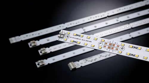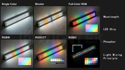
The five LED packaging technology families are DIP, SMD, COB, COG, and MIP. They are not equal in commercial importance. General lighting is dominated by SMD and COB, because both are mature, cost-effective, and well supported by supply chains. COG and MIP are mainly used for fine-pitch LED displays, while DIP survives in legacy and niche products. Each family differs in structure, working principle, strengths, and typical applications.
DIP LED Packaging.
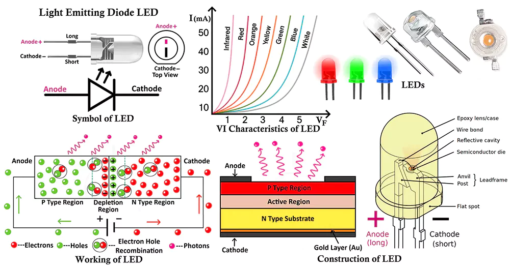
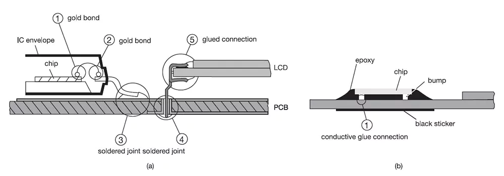
DIP (dual in-line package) is the original LED format: a die mounted on a lead frame, wire-bonded, and encapsulated in an epoxy lens body, typically 3 mm or 5 mm in diameter, with two long leads. The leads pass through holes in the PCB and are wave-soldered on the opposite side, which is why the family is also called through-hole or THT (through-hole technology) packaging.
The epoxy body acts as both protection and lens, giving DIP lamps a narrow, directed beam. Their simple construction tolerates rough handling and harsh outdoor conditions, which kept them in large-pitch outdoor displays and traffic signals long after newer packages appeared.
For new lighting designs, DIP is effectively obsolete. It cannot be assembled by standard SMT lines, wastes board area, offers limited thermal performance, and costs more per lumen than SMD. Buyers will mostly encounter DIP when maintaining older equipment or sourcing indicator lights.
SMD LED Packaging.
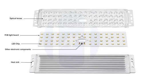
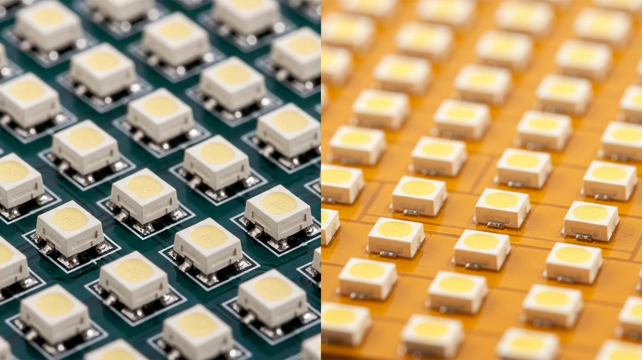
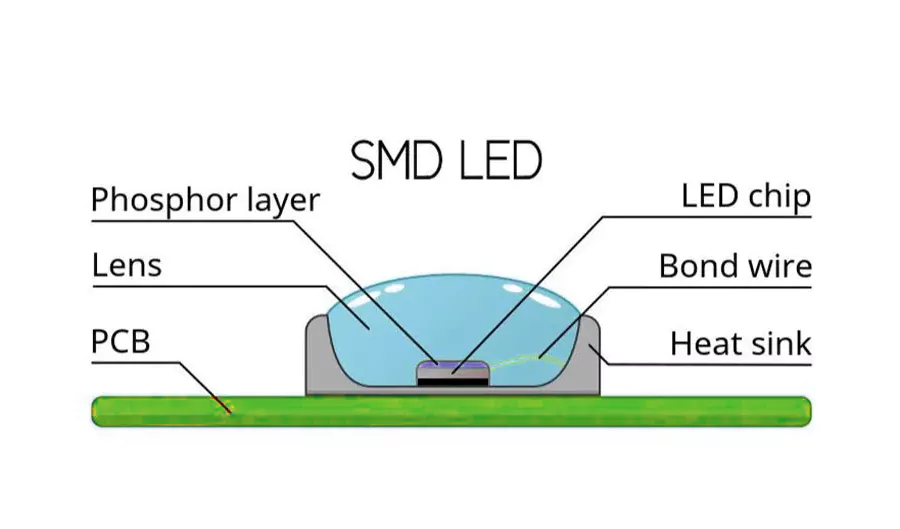
SMD (surface mount device) packaging mounts an LED die in a compact, flat package that solders directly to pads on the surface of a PCB. The package typically combines a PPA or EMC housing, a reflective cavity, metal lead-frame terminals, a wire bond or flip-chip connection, and a phosphor-loaded silicone fill. Unlike DIP, it needs no drilled holes, so reflow soldering supports automated, high-volume assembly.
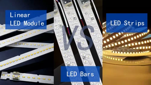
The numbers in SMD package names describe the footprint in tenths of a millimeter: a 2835 package measures 2.8 mm by 3.5 mm, while a 5050 measures 5.0 mm by 5.0 mm. Common mid-power packages such as 2835 and 3030 typically run at roughly 0.2 W to 1 W each and are widely used in bulbs, tubes, strips, panels, and LED modules. For a lighting designer, the practical advantage is flexibility: package count, spacing, color mix, and PCB layout can be adjusted to meet a target output and beam pattern.
SMD is the workhorse of general lighting for practical reasons. The supply chain is enormous and competitive, so unit cost is low. Packages are binned tightly for flux and color, which simplifies color consistency across a production run. Designs scale freely: a module designer adds or removes packages to hit a lumen target, mixes color temperatures on one board, or spaces packages to shape a beam. Individual packages can also be reworked if one fails. Market data reflects this position: Mordor Intelligence estimates SMD held about 43% of LED packaging revenue in 2025, the largest single package segment.
The trade-offs are modest per-package power and a thermal path that depends heavily on the PCB. SMD-based designs manage heat through board-level engineering: metal-core substrates, copper weight, thermal vias, and package spacing.
COB LED Packaging.
COB (chip on board) skips the individual package housing. Multiple bare LED dies are bonded directly onto a metal-core PCB or ceramic substrate, interconnected by wire bonding or flip-chip attachment, and covered together by one continuous layer of phosphor-loaded silicone. The result is a single, monolithic light-emitting surface rather than a grid of discrete points.
This structure gives COB three practical advantages. Lumen density is high, because many dies share one small area. Light output is uniform, with no visible dot pattern, which suits directional luminaires. The thermal path is short, since dies sit almost directly on the substrate. These traits make COB a common choice for downlights, spotlights, track lights, high-bay fixtures, and street lighting, and industry reporting credits COB with rapid growth in fine-pitch displays after 2023 as well.
The limitations mirror the strengths. Because all dies share one phosphor layer, a COB board delivers a single color temperature and CRI, with no per-die mixing. A failed die usually means replacing the whole board rather than reworking one component. And the concentrated emitting area demands well-designed secondary optics to
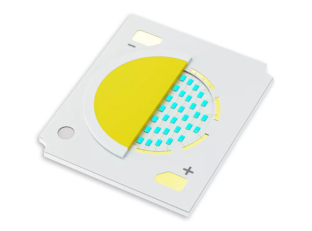
control glare. Cost per board is higher than an equivalent SMD layout, although system cost can favor COB in compact, high-output fixtures.
COG LED Packaging.
COG (chip on glass) replaces the PCB with a glass substrate. LED chips, and often their driver circuitry, are bonded directly onto glass using conductive films and transparent conductive traces such as ITO (indium tin oxide). The glass provides exceptional flatness and dimensional stability, which allows extremely fine pixel pitches that PCB-based packaging cannot reach; display industry sources describe COG as a candidate platform for Micro LED products with pitches below P0.1.
COG also enables thin and even transparent display panels, since glass needs no extra thickness for rigidity and can carry see-through conductive layers. The costs are manufacturing complexity, strict placement accuracy requirements, and a price level that keeps COG in premium display applications. COG is not a mainstream general-lighting package.
MIP LED Packaging.
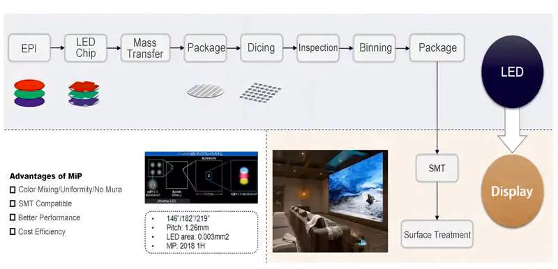
MIP (Micro LED in package) packages microscopic LED dies, typically below 100 micrometers, as discrete tested components that standard SMT lines can then mount. It answers a manufacturing problem: Micro LED displays require transferring millions of tiny dies with near-perfect yield, so MIP moves the hardest testing and binning work to the wafer level and delivers known-good micro dies in a familiar package format.
Display industry sources place MIP products in the P0.2 to P0.7 pixel pitch range and position the technology as a bridge between today’s fine-pitch displays and full Micro LED screens. MIP carries a cost premium to SMD, which confines it mainly to high-end displays. Like COG, MIP is currently concentrated in display applications rather than general lighting.
We have specifically compiled five LED module packaging technologies into a complete table. We’ve helped you differentiate between general lighting and display applications in terms of packaging technology, because buyers often encounter display-centric comparisons, and these comparisons are not applicable to module decisions for lighting fixtures.
Package | Structure | Working principle | Strengths | Limitations | Main applications |
|---|---|---|---|---|---|
DIP | Die on lead frame in epoxy lens body, through-hole leads | Wave-soldered lamp, lens shapes narrow beam | Rugged, cheap at low volumes, tolerant of harsh conditions | Obsolete for new designs; no SMT compatibility; weak thermal path | Indicators, legacy outdoor displays, traffic signals |
SMD | Die in reflective plastic housing with lead frame pads, phosphor silicone fill | Reflow-soldered discrete packages, scaled by package count | Lowest cost per lumen, huge supply chain, flexible layouts, reworkable | Limited per-package power; thermal performance depends on PCB design | Bulbs, strips, panels, LED modules, most general lighting |
COB | Bare dies bonded directly on MCPCB or ceramic under one phosphor layer | Many dies form one monolithic emitting surface | High lumen density, uniform light, short thermal path | Single CCT/CRI per board, board-level replacement, glare control needed | Downlights, spotlights, high-bay, street lighting, fine-pitch displays |
COG | Dies and drivers bonded on glass with ITO traces | Glass substrate enables ultra-fine pitch | Extreme flatness, pitch below P0.1 possible, transparent panels | High cost and process complexity | Premium and transparent displays, Micro LED research |
MIP | Micro LED dies packaged as discrete tested components | Wafer-level testing plus standard SMT mounting | Known-good micro dies, fine pitch, bridge to Micro LED | Roughly several times SMD cost | High-end fine-pitch displays |
If you are choosing between SMD and COB for a new luminaire, share the target output, footprint, and thermal conditions with us. We assess package fit together with optical design, thermal management, and manufacturability, from design review and prototyping through reliability validation and full-cycle manufacturing.
GOB (glue on board) is not an independent chip packaging form. It is a surface protection process applied on top of a finished SMD display module: a transparent epoxy or polymer resin is potted over the soldered packages and cured into a sealed protective layer. Display vendors describe the result as water, dust, impact, and static resistance at roughly IP65 level on the module face, at a cost premium of about 10% to 20% per module, with resin light transmittance around 95%.
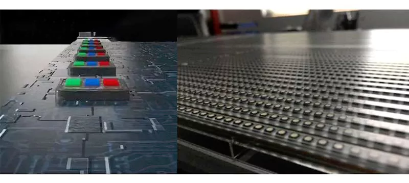
The trade-offs are harder rework, since the resin seals every package in place, and long-term questions around glue stress, heat, and potential yellowing. GOB answers a display problem: rental and public screens that are touched, bumped, and exposed to weather. General lighting achieves similar protection at the module or luminaire level with conformal coatings, potting, and sealed housings, so GOB itself rarely appears in lighting products.