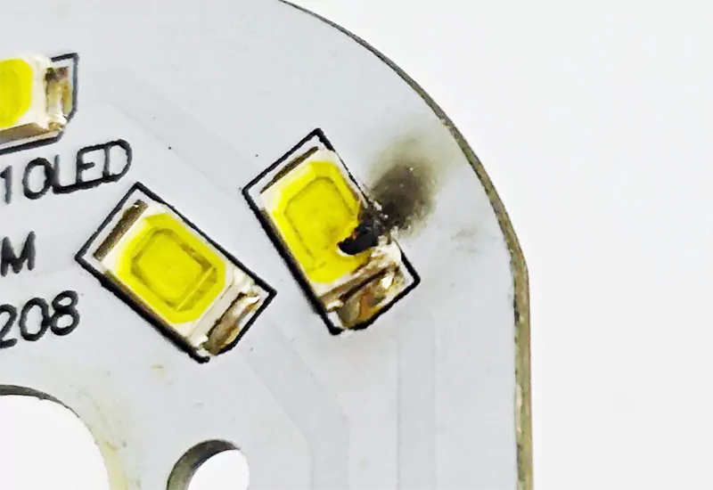
A luminaire program can pass its initial photometric review and still fail in the field. Two years in, a portion of the fixtures drift in color temperature, output slips below the lumen-maintenance target, and the warranty desk starts approving module replacements one by one. The LED Chip package itself can be the failure origin, with delamination, bond fatigue, and silver sulfidation building up silently before they surface as light loss or an open circuit.
LED package failures cluster into six mechanisms, with ESD and EOS forming a separate early-life class, and almost all of them trace back to four pressures: heat, mechanical stress, moisture or chemical exposure, and current density. Delamination and cracking come from thermal-mechanical strain; bond failure, electromigration, ESD, and EOS come from electrical and interconnect stress; sulfidation, moisture ingress, and lumen depreciation come from the environment and operating temperature. Understanding the mechanism matters because each one has a different prevention lever and a different place in the supply chain where it should be caught.
Thermal and mechanical stress: delamination and cracking.
Delamination is separation at an interface inside the package, most often between the die and phosphor, the phosphor and silicone, or the silicone and substrate. In our package review, we treat coefficient-of-thermal-expansion mismatch as the first mechanical suspect because a separated layer lengthens the heat path and raises thermal resistance. An internal study modeled thermal-mechanical stress from coefficient-of-thermal-expansion mismatch at around 255 MPa, far above the moisture-assisted stress contribution, and showed that a delaminated layer blocks the heat path and raises thermal resistance. Cracking follows the same strain logic during reflow soldering or thermal cycling, and a crack often opens a moisture channel that accelerates other failures. Prevention starts with low-CTE mold compounds and optimized leadframe design, controlled reflow profiles, and moisture-sensitive-level handling before soldering.
Interconnect and electrical stress: bond failure, electromigration, and ESD/EOS
Bond failure is fatigue of the wire bond or die attach under repeated thermal cycling. The failure often concentrates at the wire neck, while intermetallic growth and die-attach voids can further reduce the margin. Our study of 25-micrometer gold, copper, and palladium-coated copper wire bonds reported fatigue lifetimes ranging from roughly 100 to 1,000,000 cycles, depending on the applied stress and test conditions. That range should not be treated as a package lifetime guarantee. We would first confirm the wire material, bond geometry, thermal-cycle profile, and die-attach quality before comparing the result with another package.
Electromigration is the current-driven movement of metal atoms under high current density. A Nature Scientific Reports study of flip-chip solder joints described void nucleation near localized current crowding above a threshold of approximately (2.0 \times 10^4) A/cm² in the tested configuration. The result is specific to that joint design and stress condition, and the study does not establish a universal LED-package lifetime limit. We therefore treat current density, pad design, and thermal headroom as a combined review rather than using the threshold as a standalone pass/fail value.
ESD and EOS require a separate incoming and process-control screen. ESD is a transient electrostatic discharge that can create latent damage; EOS is sustained overcurrent or overvoltage that can damage the die or bond. A common mistake is to treat one ESD rating as proof of overall package reliability. Specify the applicable test method and scope, then align the component rating with driver protection, handling controls, and incoming inspection. HBM levels such as 2 kV, 4 kV, and 8 kV should not be conflated with system-level methods such as IEC 61000-4-2. In assembly, we would also control humidity, with approximately 40–60% RH as the stated process range, and verify the requirement against the actual factory procedure and test standard.
Chemical, moisture, and thermal degradation.
Silver sulfidation is the most common chemical failure: sulfur compounds react with the silver leadframe to form silver sulfide, darkening the reflector and cutting light output. A chemical-compatibility source’s chemical compatibility note estimates a 30-40% light loss from silver sulfidation, and a sulfur-corrosion source’s sulfur corrosion application note lists the three consequences: flux and color shift, wire open, and reduced reliability. Moisture acts as the electrolyte that accelerates the reaction and can also enter through non-hermetic silicone, which is why IP ratings do not equal moisture protection.
Thermal degradation is the gradual loss of output as junction temperature drives phosphor quenching, encapsulant yellowing, and lumen depreciation; it is measured and projected through the IES LM-80 and TM-21 testing standards, where lifetime is expressed as L70, L80, or L90.
That is why we treat corrosion protection as a package-level design decision, not a final assembly add-on. For sulfur-rich or humid applications, our self-developed LED packages use a zero-silver construction to improve sulfidation resistance and an APB double-layer vacuum coating to support airtightness. These choices are intended to reduce the exposure paths that can darken the reflector or accelerate moisture-related degradation, helping professional users protect light output and reliability before the package enters module engineering.
Drawing on more than 10 years of our LED chip and package development experience, we map each failure mode to its root cause, consequence, prevention lever, and the point in the supply chain where it should be caught. Read the mechanism first, then the prevention column, because most packages fail from more than one pressure acting together.
| Failure mode | Root cause | Typical consequence | Prevention lever | Where to catch it |
|---|---|---|---|---|
| Delamination | CTE mismatch and thermal-mechanical stress; moisture assists | Higher thermal resistance, reduced light extraction, accelerated decay | Low-CTE mold compound, leadframe optimization, MSL handling, controlled reflow | Incoming inspection, thermal cycling tests |
| Cracking | Reflow shock, thermal cycling, brittle aging of encapsulant | Moisture channel, light loss, open circuit | Silicone over epoxy, reflow profile control, mechanical strain relief | Reflow qualification, thermal shock tests |
| Bond failure | Wire fatigue, intermetallic growth, die-attach voids | Open circuit, intermittent operation, higher resistance | Bond pull and shear checks, copper or PCC wire selection, void-free die attach | Wire pull, ball shear, die shear tests |
| Electromigration | High current density, current crowding, joule heating | Metal migration, void growth, open circuit | Derating, lower current density, robust pad design | High-temperature operating life tests |
| Chemical and moisture ingress | Silver sulfidation, moisture as electrolyte | 30-40% light loss, color shift, wire open | Silver-free or coated leadframe, hermetic design, dry assembly | Sulfur and humidity tests, salt spray |
| Thermal degradation | High junction temperature, phosphor and silicone aging | Lumen depreciation, CCT shift, shorter L70/L90 life | Thermal management, derating, TIM quality, LM-80/TM-21 verification | Lumen maintenance testing per LM-80/TM-21 |
| ESD and EOS | Transient discharge or sustained overstress | Latent damage, dead on arrival, burned die | ESD-protected area, HBM-rated parts, driver protection, humidity control | Incoming ESD testing, burn-in |
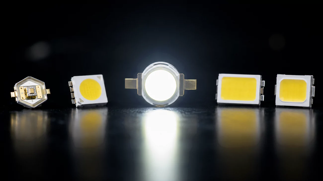
In our LED package development, we improve efficiency through four levers: light extraction, thermal management, electrical interconnection, and color conversion. The largest structural gains often come from flip-chip interconnect and low-thermal-resistance constructions because they remove wire-bond shadowing, shorten the heat path, and support the intended drive current without excessive junction temperature. These are the levers we review against a package-series datasheet before the selected light source enters module engineering.
Four levers that control light output.
At the LED package level, light output depends on the refractive index of the encapsulation materials, the reflectivity of the package structure, phosphor-conversion efficiency, and the thermal path that controls junction temperature. Electrical interconnection also affects output: wire bonds add resistance and shadowing, while flip chip can remove both. These package-level levers determine how efficiently the LED bead converts electrical input into usable light before the selected bead enters module engineering.
Materials and structures that cut losses.
High-reflectivity packaging is a materials problem with measurable targets. A materials presentation hosted by Fraunhofer ENAS describes package bodies with reflectance above 90% at 440 nm using titanium dioxide fillers, and white EMC and ceramic carriers are chosen specifically to hold reflectivity at operating temperature. Low thermal resistance is achieved structurally: an internal review reports flip-chip thermal paths that are roughly one-third to one-quarter of a vertical LED’s path, and an IMAPS conference paper (IMAPS archive) demonstrated a near-chip-scale package with junction-to-case thermal resistance below 0.6 °C/W. Flip chip also eliminates the wire bond, which removes shadowing and parasitic resistance in one step, which is why flip-chip and CSP constructions dominate high-efficacy roadmaps.
At Higntek, we develop the LED package before module engineering. For applicable AUX Series designs, we replace the silver layer with a more stable alloy, apply an APB double-layer vacuum coating to improve airtightness, and use Jet Vapor Deposition to reduce thermal resistance to about 1°C/W under the specified test conditions. Our NCSP-based package design then supports high efficacy across the intended current range.
After the LED package series, model, and working point are selected, the bead becomes an input to LED module engineering. Module work then covers PCB design, thermal management, optical design, prototyping, reliability testing, and volume production; it does not change the package-level silver-free, coating, or interconnect processes described above.